Shoot-through detector using FPGA
Posted in Embedded, FPGA By Grig On May 2, 2022This project allows to detect a shoot-through condition on digital drivers.
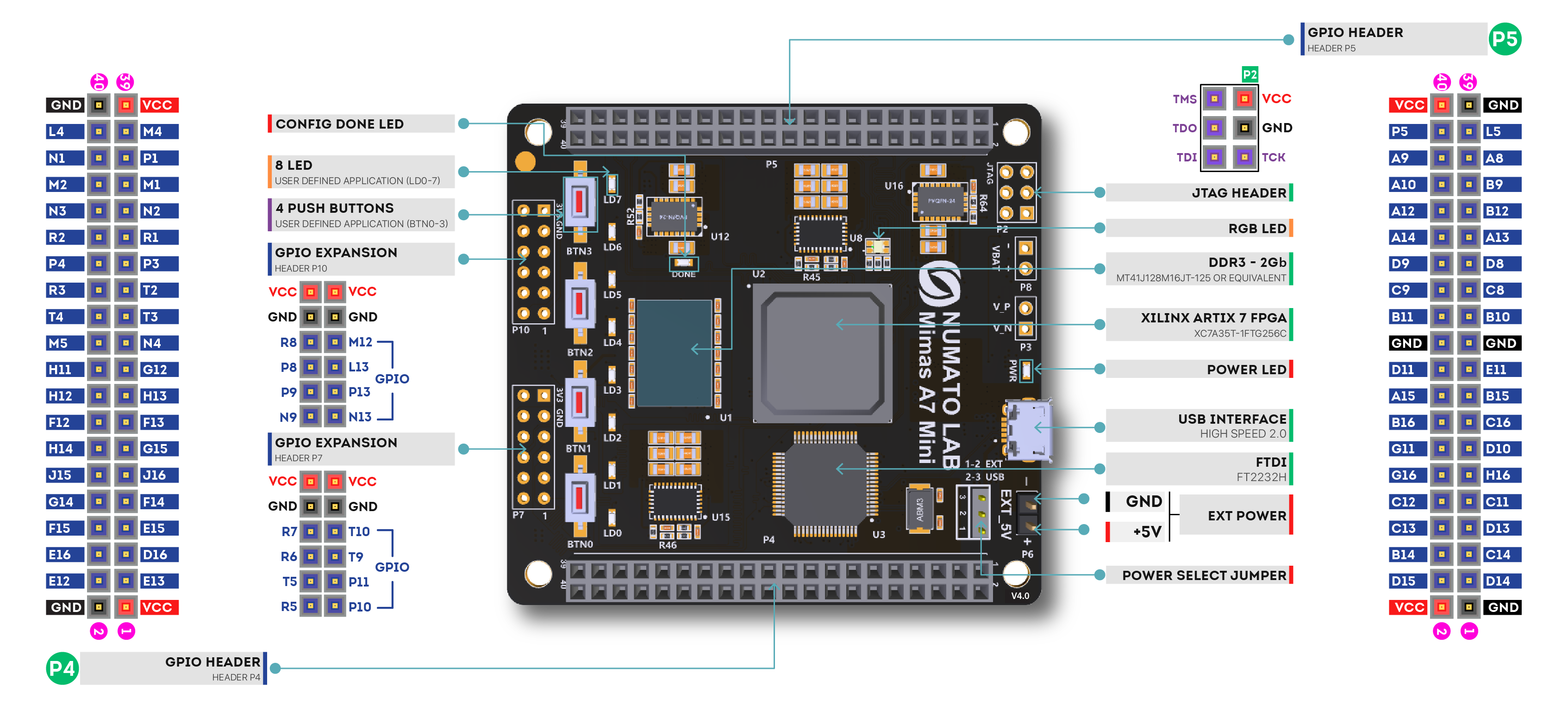
The FPGA board used is Mimas A7 Mini from Numato Lab, the code is written in Verilog and IDE is Vivado.
What is shoot-through?
In a half-bridge stage (Fig 2), if both transistors are driven simultaneously, even for a few nanoseconds, a shoot-through condition might occur (Fig 1). This occurence depends on multiple factors, like transistors sensitivity, gate voltage threshold, driver’s speed and many others, but the most important factor is the overlapping of the driving commands. The consequences of the shoot-through starts from loss of efficiency, power supply stress due to overcurrent and going up to MOSFETs destruction. The phenomena is also called cross-conduction.
What to do to avoid the shoot-through?
Simply, insert a guard time between the high-side transistor duty-cycle and the low-side one. This guard time is called a dead time (Fig 3).
Shoot-through checker
The presented project is an automatic verifier of the overlapping and near-overlapping of the two signals: the high-side drive and the low-side drive.
A simplified block diagram of the device is below (Fig 4):
Basically, the detector generates a pulse of at least 1 us every time the two input signals have a gap shorter than 100ns. The output pulse might be longer if the input signals are overlapped.

How to use the shoot-through checker?
Connect the wires to the output of the digital driver, a pair for each driver.
I.e. “driver_high” to I0.a and “driver_low” to I0.b. Or viceversa, it doesn’t matter. The detected shoot-through event is available for visualization with oscilloscope or logic analyzer on pin O0. Also, the LD0 will turn on for an indefinite anount of time to signal that a shoot-through occured. It can be cleared by pressing button BTN0.

The signalling LEDs are LD0, LD1, LD2, LD3 and the unique “clear” button is BTN0 which clears all four LED events.
Implementation details
One detection block is composed out of three monostable blocks and an AND gate (Fig 5):
The code for the detector is quite simple and is based on the monostable
module detector(input a, input b, input clk, output out);

    wire ma, mb;

    monostable mA(.in(a), .out(ma), .clk(clk));
    monostable mB(.in(b), .out(mb), .clk(clk));

    monostable #(.SIZE(7), .TIMEOUT(100)) mO (.in(ma & mb), .out(out), .clk(clk));

endmodule
The monostable role is to delay the falling edge of the input signals by a number of clocks while the rising edge remains unchanged. The monostable is briefly explained below (Fig 6):
The code for the monostable is here
module monostable(input in, input clk, output out);
	parameter SIZE = 4;
	parameter TIMEOUT = 10;

  reg [SIZE-1:0] counter;

  // fake reg
  reg [SIZE-1:0] pre_counter;

  assign out = (counter <= TIMEOUT) ? 1 : 0;

  always @(*)
    begin
      if (out)
        pre_counter = counter + 1;
      else
        pre_counter = counter;
    end


  always @(posedge clk or posedge in)
    begin
      if (in==1)
        counter <= 0;
      else
        counter <= pre_counter;
    end

endmodule
There are a few other functional blocks. The complete elaborated design of a detection block, including the input synchronizers, the output flag and clearing input is below.


The complete code is on this github repository.


